Ps5 Motherboard Diagram
Ps5 hdmi gbatemp traces repair mapped Ps5 ds4 dualsense motherboard comparison side internal teardown repairability ps4 features look mp1st dualshock Ps5 pinout chip devs psxhax
Model of ps5 hdmi filter? | GBAtemp.net - The Independent Video Game
Ps5 h2025k4702 ic flash chip pinout diagram for ps5scene devs Motherboard diagrams to print Model of ps5 hdmi filter?
Asus p5q motherboard deluxe layout manual
Ps5 dualsense teardown features repairability, internal look & ds4Ps5 teardown video: sony shows off ssd slot and other components Motherboard diagrams galleryhip via2 motherboard overview, 1 motherboard layout, motherboard overview -2 2.
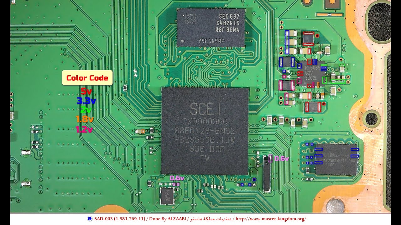
Ps5 teardown motherboard slotVoltage playstation standby nvg alzaabi Playstation 4 nvg 001 standby voltage diagrams by alzaabiInside the playstation 4: motherboard components explained.

Motherboard ps5
Standby voltage diagrams alzaabiPlaystation 4 sad-003 (1-981-769-11) standby voltage diagrams by .
.

PS5 teardown video: Sony shows off SSD slot and other components - Polygon

PS5 DualSense Teardown Features Repairability, Internal Look & DS4

Model of ps5 hdmi filter? | GBAtemp.net - The Independent Video Game

PS5 H2025K4702 IC Flash Chip Pinout Diagram for PS5Scene Devs | PSXHAX

PlayStation 4 NVG 001 Standby Voltage Diagrams By ALZAABI - YouTube

Motherboard Diagrams to Print | 101 Diagrams

Inside the PlayStation 4: Motherboard Components Explained